
Welcome to the Takenobu Lab Website
| Our research focus on p-electron materials, e.g. organic and nano-carbon materials. Our aim is to understand physical properties of these materials and to explore their novel functional devices. The current research interests include investigating transport and optical properties of carbon nanotubes, atomically thin materials, and conducting polymers. We also focus on device applications using these materials, such as transistors, thermoelectric devices, light-emitting (photo-detecting) devices, and lasers. If you are interested in our group, please contact us. We always welcome domestic/international JSPS research fellows. Please see the following website for further information: more info |
Contact Information
Professor Taishi Takenobu, CV and publications
Furo-cho, Chikusa-ku, Nagoya 464-8603 JAPAN
Department of Applied Physics
School of Engineering
Nagoya University (Location and Access)
Building 3, Room 261
TEL:+81-52-789-5173 FAX:+81-52-789-3712
MAIL: ![]()
Current projects in the lab
Novel functional Materials
Novel materials can create new physics and new electronics. And, sometime, they change our daily life drastically. We are trying for exploring novel functional materials to open new world.
Related papers: Phys. Rev. Lett. 2010, Nat. Mater. 2004, Nat. Mater. 2003
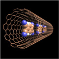
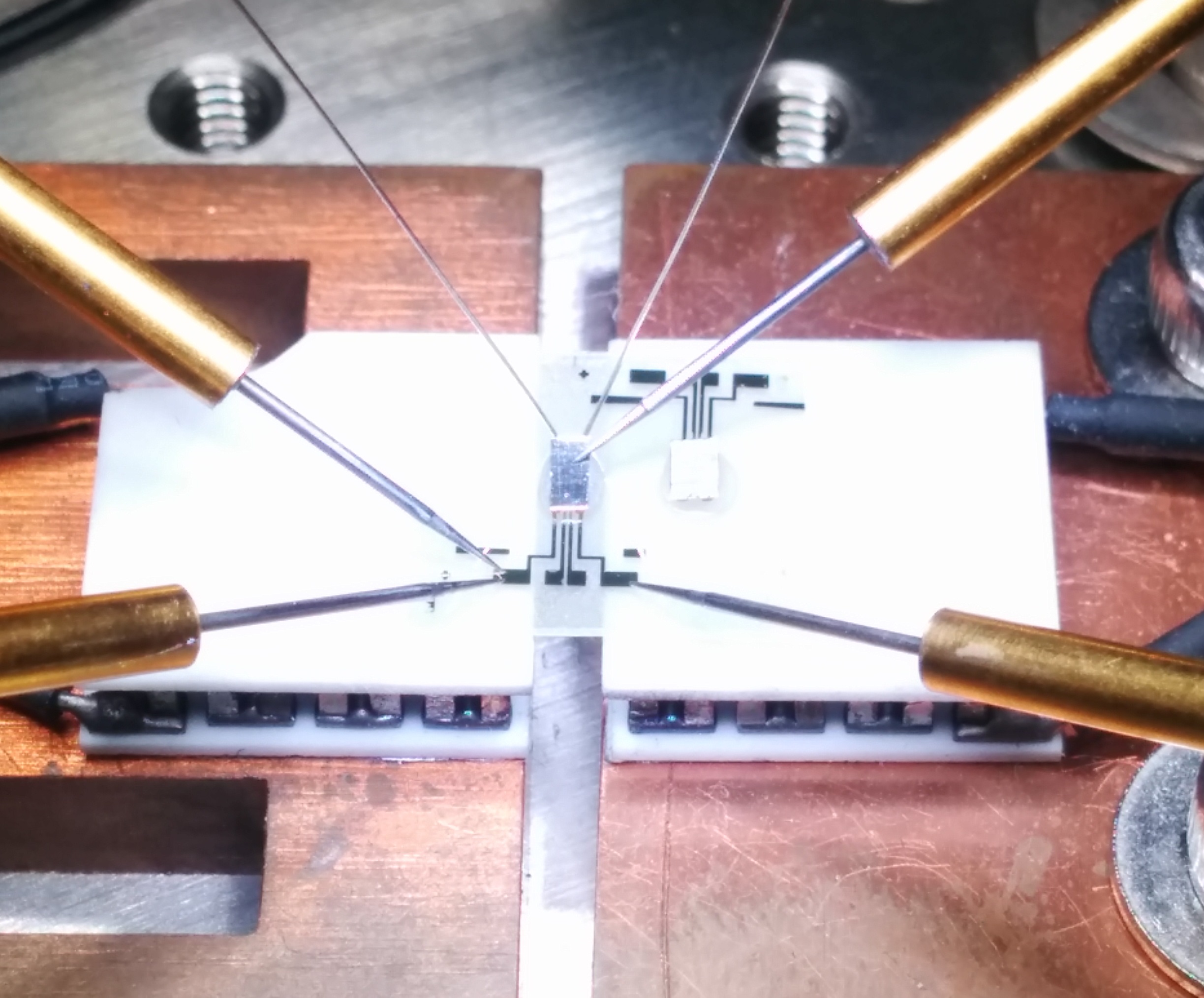
Physical properties and devices of atomically thin materials
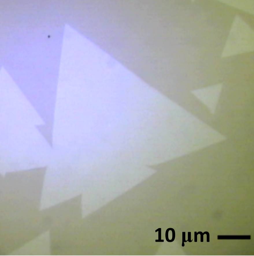
Atomically thin materials, such as graphene, show drastic evolutions in their physical properties compared to conventional solids. We are investigating unique electronic and optical properties of these materials and exploring their new functionalities.
Related papers: Adv. Mater. 2017, Phys. Rev. Lett. 2016, ACS Nano 2014
Physical properties and devices of conducting polymers
Conducting polymers are attracting much attentions as new electronic materials. We are trying to reveal fundamental tranport and spintronic properties of conducting polymers to demonstrate their electronic and thermoelectric devices.
Related papers: Nat. Mater. 2016, Adv. Mater. 2014, Appl. Phys. Exp. 2015
Electrically driven organic laser
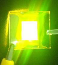
One of the biggest advantages of organic materials is an excellent luminescent property, which is well known in organic light-emitting diode. However, the electrical driven organic lasers have not yet been realized. We are trying to realize first electrical driven organic laser.
Related papers: Adv. Mater. 2017, Sci. Rep. 2015, Phys. Rev. Lett. 2008
Pressure-induced new physical properties in organic materials
Organic materials are soft materials, and it allows us to control their electronic and magnetic properties via pressure (and strain). We are trying to establish new method for tuning electronic phase of organic materials by pressure control.
Related papers: Nat. Phys. 2015, Phys. Rev. B 2016, Nat. Commun 2016
Flexible Electronics/Printed Electronics
Nanomaterials and organic materials have flexibility and printability. Such unique mechanical properties might create new functional electronics. We are trying to realize flexible and/or printed devices based on these materials using unique device structure and fabrication process.
Related papers: Adv. Mater 2009, Nano Lett. 2012, Adv. Mater. 2010